

OB-216 Modbus Interface Reference
OB-216 Settings
Section titled “OB-216 Settings”Table – OB-216 Settings
Setting operating modes (Address 100)
| Parameter | Value range | Factory value | Type | W/R | Address (DEC) |
|---|---|---|---|---|---|
| Operating mode | 0…6, 8, 11–12 | 1 | UINT | W/R | 100 |
Operating mode values:
- Measurement of discrete signals:
- 0 – impulse counter (discrete signal)
- 1 – logical input
- Measurement of analog signals:
- 2 – voltage measurement
- 3 – current measurement
- Temperature measurement:
- 4 – NTC sensor (10KB)
- 5 – PTC 1000 sensor
- 6 – PT 1000 sensor
- Additional:
- 8 – digital sensor (1-Wire)*
- 11 – pulse counter (voltage)
- 12 – pulse counter (current)
Connected digital sensor (Address 101)
| Parameter | Value range | Factory value | Type | W/R | Address (DEC) |
|---|---|---|---|---|---|
| Connectable digital sensor | 0…3 | 0 | UINT | W/R | 101 |
Connectable digital sensor values:
- 0 – DS18B20 (1-Wire)
- 1 – DHT11 (1-Wire)
- 2 – DHT21/AM2301 (1-Wire)
- 3 – DHT22 (1-Wire)
Temperature and threshold settings (Addresses 102–105)
| Parameter | Value range | Factory value | Type | W/R | Address (DEC) |
|---|---|---|---|---|---|
| Temperature correction | –99…99 | 0 | INT | W/R | 102 |
| Working parameter* | 0…1 | 0 | UINT | W/R | 103 |
| Upper threshold | -32767…32767 | 250 | INT | W/R | 104 |
| Lower threshold | –32767…32767 | 0 | INT | W/R | 105 |
Working parameter values:
- 0 – temperature
- 1 – humidity
Settings for the pulse counter (Addresses 106–108)
| Parameter | Value range | Factory value | Type | W/R | Address (DEC) |
|---|---|---|---|---|---|
| Pulse counter mode | 0…2 | 0 | UINT | W/R | 106 |
| Contact debouncing delay** | 1…250 | 10 | UINT | W/R | 107 |
| Number of pulses per counting device*** | 1…65534 | 8000 | UINT | W/R | 108 |
Pulse counter mode values:
- 0 – counter on the rising edge of the pulse
- 1 – counter on the falling edge of the pulse
- 2 – counter on both pulse edges
Data transfer settings (Addresses 109–116)
| Parameter | Value range | Factory value | Type | W/R | Address (DEC) |
|---|---|---|---|---|---|
| RS-485 protocol | 0…1 | 0 | UINT | W/R | 109 |
| MODBUS UID | 1…247 | 28 | UINT | W/R | 110 |
| Exchange rate | 0…8 | 3 | UINT | W/R | 111 |
| Parity and stop bits control | 0…2 | 0 | UINT | W/R | 112 |
| Interface selection | 0…2 | 0 | UINT | W/R | 113 |
| Password protection Modbus**** | 0…1 | 0 | UINT | W/R | 116 |
| Modbus password value | A–Z, a–z, 0–9 | admin | STRING | W/R | 117–124 |
RS-485 protocol values:
- 0 – MODBUS RTU
- 1 – MODBUS ASCII
Exchange rate values:
- 0 – 1200
- 1 – 2400
- 2 – 4800
- 3 – 9600
- 4 – 14400
- 5 – 19200
- 6 – 38400
- 7 – 57600
- 8 – 115200
Parity and stop bits control values:
- 0 – no, 2 stop bits
- 1 – even, 1 stop bit
- 2 – odd, 1 stop bit
Interface selection values:
- 0 – automatically
- 1 – RS-485
- 2 – USB
Measured value conversion settings (Addresses 130–134)
| Parameter | Value range | Factory value | Type | W/R | Address (DEC) |
|---|---|---|---|---|---|
| Measured value conversion | 0…1 | 0 | UINT | W/R | 130 |
| Minimum input value | 0…2000 | 0 | UINT | W/R | 131 |
| Maximum input value | 0…2000 | 1000 | UINT | W/R | 132 |
| Minimum converted value | –32767…32767 | 0 | INT | W/R | 133 |
| Maximum converted value | –32767…32767 | 1000 | INT | W/R | 134 |
Measured value conversion values:
- 0 – conversion is disabled
- 1 – conversion is enabled
Settings for analog output (Addresses 150–156)
| Parameter | Value range | Factory value | Type | W/R | Address (DEC) |
|---|---|---|---|---|---|
| Analog output control | 0…4 | 0 | UINT | W/R | 150 |
| Register for writing value in manual mode | 0…2000 | 0 | UINT | W/R | 151 |
| Converting the manual control value to analog signal | 0…1 | 0 | UINT | W/R | 152 |
| Minimum input value | –500…2500 | 0 | INT | W/R | 153 |
| Maximum input value | –500…2500 | 1000 | INT | W/R | 154 |
| Minimum converted analog value | 0…2000 | 0 | UINT | W/R | 155 |
| Maximum converted analog value | 0…2000 | 1000 | UINT | W/R | 156 |
Analog output control values:
- 0 – control is disabled
- 1 – automatic control of voltage output
- 2 – automatic control of current output
- 3 – manual control of voltage output
- 4 – manual control of current output
Converting the manual control value to analog signal values:
- 0 – conversion is disabled
- 1 – conversion is enabled
Notes:
- * Used parameter of the selected digital sensor (address 101).
- ** Delay in milliseconds used to suppress contact bounce in the «Pulse counter» and «Logic input/pulse relay» modes.
- *** Used only if pulse counter is enabled. The «Value» column indicates the number of pulses at the input, after the registration of which the counter is increased by one. Writing to memory is performed at intervals of 1 minute.
- **** If «Modbus password protection» is enabled (address 116 value «1»), then the correct password value must be written to addresses 51-58 in order to access the writing functions to the other addresses.
Command Registers
Section titled “Command Registers”| Name | Description | W/R | Address (DEC) |
|---|---|---|---|
| Command register | see Command codes below | W/R | 50 |
| Entering Modbus password (8 ASCII characters) | Set the correct password to access the recording functions (default value is “admin”). To disable recording functions, set any value other than a password. Allowed characters: A-Z; a-z; 0-9 | W/R | 51 – 58 |
Notes:
- W/R – type of access to the register write/read;
- an address like “50” means a 16-bit value (UINT);
- address like “51 – 58” mean a range of 8-bit values.
Command codes
| Code | Purpose |
|---|---|
| 18220 | write settings to flash memory |
| 18263 | load settings from flash memory |
| 42228 | device restart |
| 41672 | reset to factory settings |
| 61989 | reset the impulse counter (this will clear all values stored in the flash memory) |
Additional Registers
Section titled “Additional Registers”| Name | Description | W/R | Address (DEC) |
|---|---|---|---|
| Identifier | Device ID (value 28) | R | 0 |
| Firmware version | 12 | R | 1 |
| Impulse counter | – | W/R | 4:5 |
| Measured value* | – | R | 6 |
| Temperature (× 0.1°С) | – | R | 11 |
| Humidity (× 0.1%) | – | R | 12 |
| Converted value** | – | R | 16 |
| Converted analog value*** | – | R | 17 |
Notes:
- address of the form «1» means the value of 16 bits (INT);
- address of the form «2:3» means 32-bit value (ULONG);
- * Measured value from analog sensors (voltage, current, temperature);
- ** Converted value of the measured value in accordance with the settings in the registers (addresses 131 - 134);
- *** The measured value converted into an analog signal at the output in accordance with the settings in the registers (addresses 153 - 156)
Status Register (Address 2:3)
Section titled “Status Register (Address 2:3)”| Name | Description | W/R | Address (DEC) |
|---|---|---|---|
| Status register | see Status bits below | R | 2:3 |
Status bits:
| Bit | Description | Equals 0 | Equals 1 |
|---|---|---|---|
| bit 0 | impulse counter (discrete) | disabled | enabled |
| bit 1 | counter on the leading edge of the pulse | disabled | on |
| bit 2 | counter on the trailing edge of the pulse | disabled | on |
| bit 3 | counter on both pulse edges | disabled | on |
| bit 4 | logical input | disabled | enabled |
| bit 5 | voltage measurement | disabled | enabled |
| bit 6 | current measurement | disabled | enabled |
| bit 7 | measurement by the NTC (10KB) sensor | disabled | enabled |
| bit 8 | measurement by PTC1000 sensor | disabled | enabled |
| bit 9 | measurement by PT1000 sensor | disabled | enabled |
| bit 10 | impulse counter (by voltage) | disabled | enabled |
| bit 11 | impulse counter (by current) | disabled | enabled |
| bit 12 | measurement by DS18B20 sensor | disabled | on |
| bit 13 | measurement by DHT11 sensor | disabled | on |
| bit 14 | measurement by DHT21 sensor | disabled | on |
| bit 15 | measurement by DHT22 sensor | disabled | on |
| bit 16 | automatic output mode | for voltage | for current |
| bit 17 | manual output mode | for voltage | for current |
| bit 18 | «IO2» input | open | closed |
| bit 19 | exchange interface | RS-485 | USB |
| bit 20 | overvoltage | no | detected |
| bit 21 | undervoltage | no | detected |
| bit 22 | overcurrent | no | detected |
| bit 23 | undercurrent | no | detected |
| bit 24 | temperature high | no | detected |
| bit 25 | temperature low | no | detected |
| bit 26 | humidity high | no | detected |
| bit 27 | humidity low | no | detected |
| bit 28 | voltage/current input value conversion | disabled | enabled |
| bit 29 | device settings changes | saved | not saved |
| bit 30 | device calibration | calibrated | uncalibrated |
| bit 31 | analog output value conversion | disabled | enabled |
Configuring the Device for USB Operation
Section titled “Configuring the Device for USB Operation”If the register (address 113) contains the value «0» (automatic selection of the interface), the device will automatically switch and work with USB, while OB-216 is connected to the PC via a USB cable (the RS-485 interface is unavailable while it does). Otherwise, if the cable is disconnected, the device works with the RS-485 interface.
To work with the RS-485 interface only , it is necessary to write the value «1», to the register (address 113); with this setting, the device will not switch to work with USB when the cable is connected.
To work with the USB interface only, it is necessary to write the value «2», to the register (address 113), with this setting the device will work only with the USB interface, and access to the device via RS-485 will be prohibited.
Modbus protocol usage
Section titled “Modbus protocol usage”OB-216 allows data exchange with external devices using the Modbus protocol with a limited set of commands (the list is given in List of Supported Functions).
When building a network, the bus topology and master-slave organization is used, where OB-216 acts as a slave. Only one master can be present on the network with one or several slaves. A personal computer software or a programmable logic controller usually acts as a master node.
With this organization, only the master node can act as the initiator of exchange cycles. Host requests are individual (addressed to a specific device). OB-216 transmits in response to individual requests from the master.
If errors are detected in receiving requests, or if it is impossible to execute the received command, OB-216, as a response, generates an error message.
The addresses (in decimal) of the settings registers and their purpose are shown in Settings Registers.
The addresses (in decimal) of the command registers, commands and their purpose are shown in Command Registers.
Addresses (in decimal) of additional registers and their purpose are given in Additional Registers.
The address (in decimal) of the status register and its purpose is given in Status Register.
List of Supported Functions
Section titled “List of Supported Functions”| Function (hex) | Appointment | Note |
|---|---|---|
| 0x03 | Reading one or more registers | Maximum 50 |
| 0x06 | Writing one value to a register | – |
| 0x08 | Communication diagnostics | – |
Message Formats
Section titled “Message Formats”The exchange protocol has clearly defined message formats. Compliance with the formats ensures the correctness and stability of the network.
Byte Format
Section titled “Byte Format”OB-216 is configured to operate with one of two formats of data bytes: with parity control (Figure 4) and without parity control (Figure 5). In parity control mode, the type of control is also indicated: Even or Odd. Transmission of data bits is performed by the least significant bits forward. By default (during manufacture) the device is configured to operate without parity control and with two stop bits.
Byte transfer is performed at speeds of 1200, 2400, 4800, 9600, 14400 and 19200 bps. By default, during manufacturing, the device is configured to operate at a speed of 9600 bps.
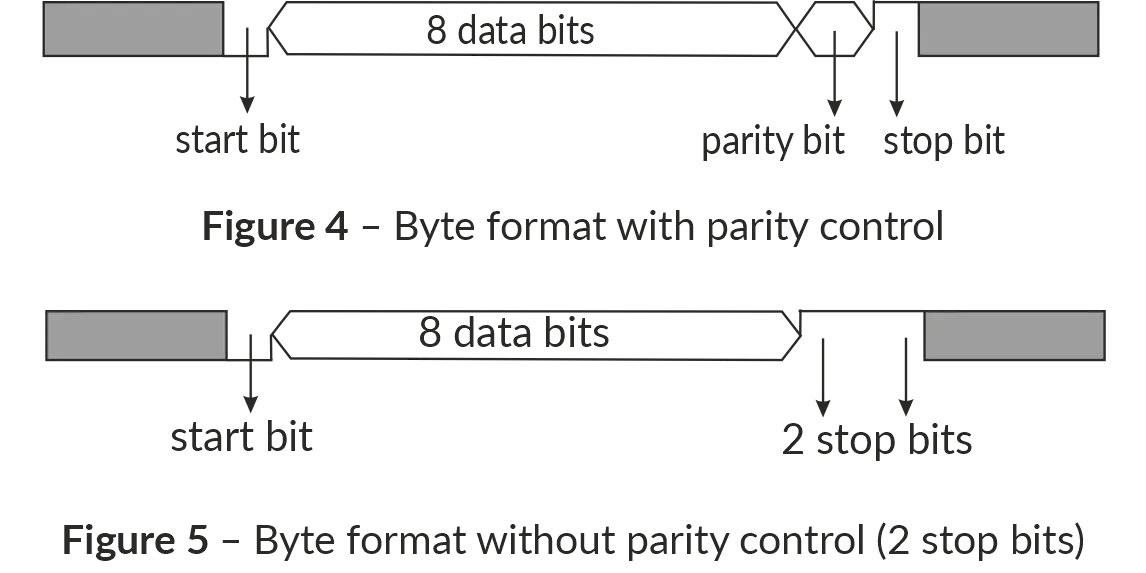
Figure 4, 5 – Byte format with parity control (top) and without parity control (bottom)
Frame Format
Section titled “Frame Format”The frame length cannot exceed 256 bytes for Modbus RTU and 513 bytes for Modbus ASCII.
In Modbus RTU mode the start and end of the frame are monitored by silence intervals of at least 3.5 bytes. The frame must be transmitted as a continuous byte stream. The correctness of frame acceptance is additionally controlled by checking the CRC checksum in the last two bytes.
The RTU address field occupies one byte. The addresses of the slaves are in the range from 1 to 247.
Figure 6 shows the RTU frame format.
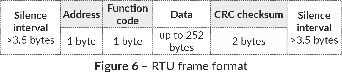
Figure 6 – RTU frame format
In Modbus ASCII mode the start and end of the frame are controlled by special characters:
- symbol
:(0x3A) – for start of the frame; - symbols
\r\norCR+LF(0x0D,0x0A) – for the end of the frame.
The frame must be transmitted as a continuous stream of hexadecimal characters. As the frame is bounded by special characters, the timings of the transmissions are not as strict as those for RTU frame. The correctness of frame acceptance is additionally controlled by checking the LRC checksum in the last two transmitted hexadecimal characters.
The address field occupies two hexadecimal characters. The addresses of the slaves are in the range from 1 to 247.
Figure 7 shows the ASCII frame format.
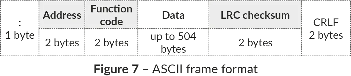
Figure 7 – ASCII frame format
Checksum Generation and Verification
Section titled “Checksum Generation and Verification”The transmitting device generates a checksum for all bytes of the transmitted message. OB-216 similarly generates a checksum for all bytes of the received message and compares it with the checksum received from the transmitting device. If the generated and received checksums do not match, an error message is generated.
CRC Checksum Generation
Section titled “CRC Checksum Generation”The checksum in the message is sent by the least significant byte forward. It is a cyclic redundant code verification based on the irreducible polynomial 0xA001.
Subroutine for CRC checksum generation in C language:
uint16_t GenerateCRC(uint8_t *pSendRecvBuf, uint16_t uCount){ const uint16_t Polynom = 0xA001; uint16_t crc = 0xFFFF; uint16_t i; uint8_t byte; for(i=0; i<(uCount-2); i++){ crc = crc ^ pSendRecvBuf[i]; for(byte=0; byte<8; byte++){ if((crc & 0x0001) == 0){ crc = crc >> 1; }else{ crc = crc >> 1; crc = crc ^ Polynom; } } } return crc;}LRC Checksum Generation
Section titled “LRC Checksum Generation”The checksum in the message is transmitted by the most significant byte forward, which is a longitudinal redundancy check.
Subroutine for LRC checksum generation in C language:
uint8_t GenerateLRC(uint8_t *pSendRecvBuf, uint16_t uCount){ uint8_t lrc = 0x00; uint16_t i; for(i=0; i<(uCount-1); i++){ lrc = (lrc + pSendRecvBuf[i]) & 0xFF; } lrc = ((lrc ^ 0xFF) + 2) & 0xFF; return lrc;}Command System
Section titled “Command System”Function 0x03 – Reading a Group of Registers
Section titled “Function 0x03 – Reading a Group of Registers”Function 0x03 provides reading of the contents of registers OB-216. The master query contains the address of the initial register, as well as the number of words to read.
The OB-216 response contains the number of bytes to return and the requested data. The number of registers returned is limited to 50. If the number of registers in the query exceeds 50 (100 bytes), the response is not divided into frames.
An example of the query and response in Modbus RTU is shown in Figure 8.
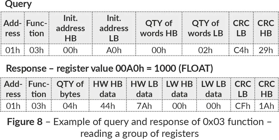
Figure 8 – Example of reading registers (Function 0x03)
Function 0x06 – Recording the Register
Section titled “Function 0x06 – Recording the Register”The function 0x06 provides recording in one OB-216 register. The master query contains the address of the register and the data to be written.
The device response is the same as the master query and contains the register address and the set data. An example of the query and response in Modbus RTU mode is shown in Figure 9.
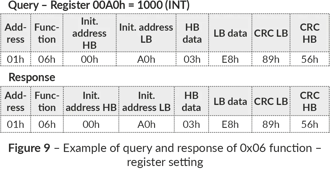
Figure 9 – Example of writing to a register (Function 0x06)
Function 0x08 – Communication Diagnostics
Section titled “Function 0x08 – Communication Diagnostics”Subfunction 0x00 - returns the received data, the response is identical to the request.
An example of a request and response is shown in Figure 10.
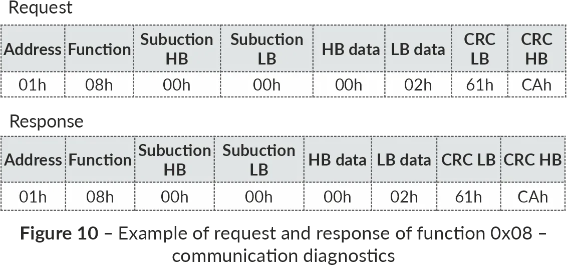
Figure 10 – Example of communication diagnostics (Function 0x08)
Modbus Error Codes
Section titled “Modbus Error Codes”| Error code | Name | Comments |
|---|---|---|
| 0x01 | ILLEGAL FUNCTION | Illegal function number |
| 0x02 | ILLEGAL DATA ADDRESS | Incorrect address |
| 0x03 | ILLEGAL DATA VALUE | Invalid data |
| 0x04 | SERVER DEVICE FAILURE | Failure of controller equipment |
| 0x05 | ACKNOWLEDGE | Data is not ready |
| 0x06 | SERVER DEVICE BUSY | System is busy |
| 0x08 | MEMORY PARITY ERROR | Memory error |